
The DDU18-series device is an 8-tap digitally buffered delay line. The signal input (IN) is reproduced at the outputs (T1-T8), shifted in time by an amount determined by the device dash number. For dash numbers less than 16, the total delay of the line is measured from T1 to T8. The nominal tap-to-tap delay increment is given by one-seventh of the total delay, and the inherent delay from IN to T1 is nominally 2.0ns. For dash numbers greater than or equal to 16, the total delay of the line is measured from IN to T8. The nominal tap-to-tap delay increment is given by one-eighth of this number.
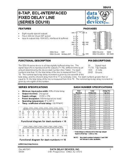
The DDU18 series provides eight equally spaced, digitally buffered outputs (T1‑T8) with a selectable total delay ranging from 4 ns to 200 ns. The device is ECL‑level compatible, available in commercial and military DIP or SMD packages, and includes a stable power‑supply bypass recommendation for repeatable performance.
Technical data include minimum input pulse width, output rise time, supply voltage range, power dissipation, operating temperature, and temperature coefficient of delay. Absolute maximum ratings and DC electrical characteristics are listed, along with package dimensions and test conditions for automated verification.
| Minimum input pulse width | 40% of total delay |
|---|---|
| Output rise time | 2 ns typical |
| Supply voltage range | -7.0 V to 0.3 V |
| Power dissipation (no load) | 50 mW typical |
| Operating temperature | 0 °C to 85 °C |
| Temp. coefficient of total delay | 100 ppm/°C |
A 0.1 µF capacitor from VEE to GND placed as close as possible to the VEE pin.
The device can tolerate a supply voltage (VEE) between –7.0 V and +0.3 V.