
This document describes a product with mechanical specifications of 110.0(W) x 22.0(H) x 10.0(Max.)(D) mm, suitable for LTM08C351 TFT module, and weighing approximately 25g. The document also provides absolute maximum ratings and electrical specifications, such as input voltage, operating temperature, input current, etc.
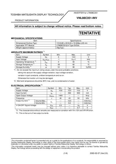
The VNL08C351 inverter is designed for the LTM08C351 (8.4" SVGA) TFT module. It supplies a typical 12.0 V input and delivers up to 50 kHz switching frequency, with detailed mechanical and electrical specifications listed.
The document includes a dimensional outline of 110 mm × 22 mm × 10 mm, absolute maximum ratings, typical supply voltage, input current, operating temperature range, and a full connector pin assignment for interfacing the inverter to the display module.
| Dimensional Outline (Typical) | 110 mm × 22 mm × 10 mm |
|---|---|
| Typical Supply Voltage (Vin) | 12.0 V |
| Typical Input Current | 900 mA |
| Typical Switching Frequency | 45 kHz |
| Operating Temperature Range | 0 °C to 50 °C |
| Storage Temperature Range | -20 °C to 60 °C |
| Storage Humidity Range | 10 % to 90 % RH |
The typical supply voltage (Vin) is 12.0 V.
The inverter operates from 0 °C up to 50 °C.
It is compatible with the LTM08C351 (8.4" SVGA) TFT module.
Pin 1 and Pin 2 provide Vin (12.0 V typical), Pin 3 and Pin 4 are GND, Pin 5 is ON/OFF, Pin 6 and Pin 7 are VR (potentiometer connections), and Pin 8 is the warning signal (5 V).