
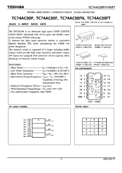
The TC74AC00 series is a high‑speed CMOS 2‑input NAND gate featuring low power consumption (typical 44 µA at 25 °C) and high noise immunity. It operates over a wide supply voltage range of 2.0 V to 5.5 V and provides symmetrical output impedance for reliable driving of transmission lines.
The device is offered in multiple packages (DIP‑14, SOP‑14, SOP‑14‑FN, TSSOP‑14) with typical weights ranging from 0.06 g to 0.96 g. Absolute maximum ratings include a supply voltage of –0.5 V to 7.0 V and a power dissipation of up to 500 mW for the DIP package. The datasheet also outlines recommended operating conditions, electrical characteristics, and usage restrictions for safety‑critical applications.
| Typical Propagation Delay (tog) | 3.8 ns (typ.) |
|---|---|
| Supply Voltage (recommended) | 2.0 V – 5.5 V |
| Power Dissipation (max, DIP) | 500 mW |
| Typical Weight (DIP package) | 0.96 g |
The typical propagation delay is about 3.8 ns.
The recommended supply voltage range is 2.0 V to 5.5 V.
The DIP package can dissipate up to 500 mW.
Yes, it is not intended for safety‑critical or high‑reliability applications such as medical, aerospace, or traffic‑signal equipment.