
This document introduces the application notes of DD-2864BY-2A OLED display module, including EVK board schematic, symbol definition, timing characteristics, connection method, etc.
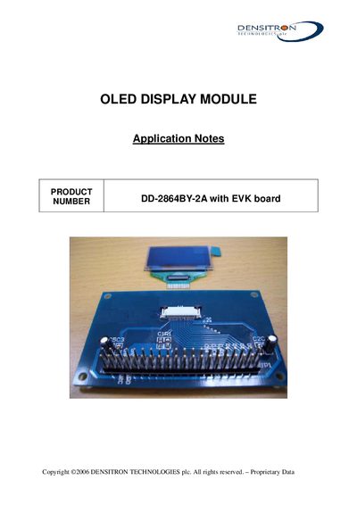
The document describes the EVK schematic, pin assignments, and 8080‑parallel interface for the DD-2864BY-2A OLED display module. It includes timing specifications, connection diagrams, and recommended initialization code for use with a host MCU.
Additional sections cover symbol definitions, detailed timing parameters, wiring between the OLED and EVK board, and a complete C‑style initialization routine to configure display settings such as contrast, duty cycle, and COM output direction.
| Supply Voltage (VDD) | 2.4 V to 3.5 V |
|---|---|
| Operating Temperature (TA) | -40 °C to 85 °C |
| Clock Cycle Time | 300 ns |
| Address Setup Time | 0 ns |
| Address Hold Time | 0 ns |
| Write Data Setup Time | 40 ns |
| Write Data Hold Time | 15 ns |
| Read Data Hold Time | 20 ns |
| Output Disable Time | 70 ns |
| Access Time | 140 ns |
| Chip Select Low Pulse Width (read) | 120 ns |
| Chip Select Low Pulse Width (write) | 60 ns |
| Chip Select High Pulse Width (read) | 60 ns |
| Chip Select High Pulse Width (write) | 60 ns |
| Rise Time | 15 ns |
| Fall Time | 15 ns |
The module operates with a VDD supply between 2.4 V and 3.5 V.
DO0‑DO7 are the 8‑bit bi‑directional data bus, and the control pins are RD#, WR#, D/C#, RES#, CS#, VCC, VDD, VSS, VCOMH, and NC.
The write data setup time is specified as 40 ns.