
This datasheet provides the characteristics parameters of APT30M75BFLL and APT30M75SFLL, including drain-source breakdown voltage, drain current, drain-source on-state resistance, zero gate voltage drain current, zero gate voltage drain current (TC=125°C), gate-source leakage current and gate threshold voltage.
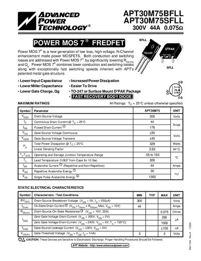
The APT30M75BFLL and APT30M75SFLL are low‑loss, high‑voltage N‑channel enhancement mode power MOSFETs featuring reduced on‑resistance, low input and Miller capacitance, and fast switching speeds. They are offered in TO‑247 or surface‑mount DPAK packages and include a fast‑recovery body diode.
Key specifications include a 300 V drain‑source breakdown voltage, 44 A continuous drain current, 176 A pulsed drain current, 329 W total power dissipation, and an on‑state resistance of 0.075 Ω. Detailed static, dynamic, thermal, and diode characteristics are provided along with typical performance curves.
| Drain‑Source Voltage (VDS) | 300 V |
|---|---|
| Continuous Drain Current (ID) | 44 A |
| Pulsed Drain Current (ID(pulse)) | 176 A |
| Gate‑Source Voltage (VGS) Continuous | +30 V |
| Gate‑Source Voltage (VGS) Transient | +40 V |
| Total Power Dissipation (PD) | 329 W |
| On‑State Resistance (RDS(on)) | 0.075 Ω |
| Input Capacitance (Ciss) | 3018 pF |
| Output Capacitance (Coss) | 771 pF |
| Total Gate Charge (Qg) | 57 nC |
The maximum drain‑source breakdown voltage is 300 V.
The device is rated for a continuous drain current of 44 A at 25 °C.
The on‑state resistance is 0.075 Ω measured at VGS = 10 V and ID = 22 A.
The continuous gate‑source voltage rating is +30 V, with a transient rating of +40 V.