
AD5302/AD5312/AD5322 is a dual rail-to-rail voltage output 8-/10-/12-bit DAC with a power supply range of +2.5V to +5.5V. It features micropower operation, power-down mode, double-buffered input logic, etc.
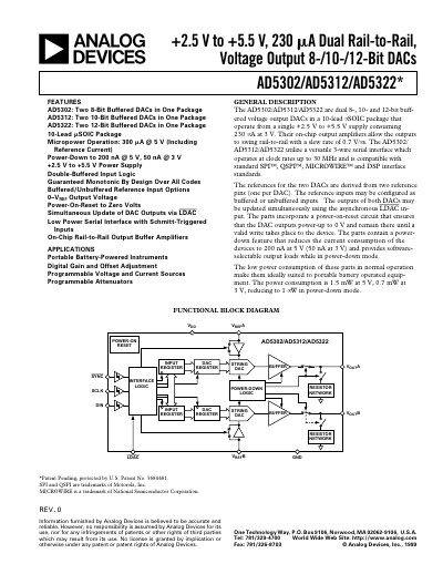
The AD5302/AD5312/AD5322 family are dual 8‑, 10‑ and 12‑bit buffered voltage‑output DACs in a 10‑lead mSOIC package. They operate from a single +2.5 V to +5.5 V supply, provide rail‑to‑rail output swing, and feature a low‑power serial interface compatible with SPI, QSPI and MICROWIRE standards. Each DAC has an independent reference input that can be buffered or unbuffered, and the devices include power‑on‑reset and programmable power‑down modes.
Key specifications include a 0.7 V/ms slew rate, up to 30 MHz serial clock, 1.5 mW typical power consumption at 5 V, and a short‑circuit current rating of 50 mA. The datasheet provides detailed electrical characteristics, timing diagrams, pin functions, and typical performance graphs for designers.
| Supply Voltage Range | +2.5 V to +5.5 V |
|---|---|
| Slew Rate | 0.7 V/ms |
| Maximum Serial Clock Rate | 30 MHz |
| Power Consumption (Normal Mode) | 1.5 mW at 5 V, 0.7 mW at 3 V |
| Short‑Circuit Output Current | 50 mA |
They operate from a single supply of +2.5 V to +5.5 V.
The devices can source up to 50 mA in a short‑circuit condition.
The output buffer amplifiers have a slew rate of 0.7 V/ms.
The serial interface can operate at clock rates up to 30 MHz.