
ICminer.com is the world's leading electronic components information service provider, providing comprehensive, reliable electronic components database, including price, inventory, model, data sheet, etc.
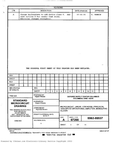
This document defines the scope, device types, case outlines, lead finishes and classification levels (Q, V, M) for the OP‑37 high‑speed, low‑noise operational amplifiers. It lists the applicable military specifications, standards and handbooks that govern the design and qualification of these microcircuits.
Detailed electrical performance characteristics are given, including absolute maximum ratings, recommended operating conditions, and typical parameter limits such as input offset current, bias current, CMRR, voltage gain, output swing, power dissipation and slew rate. A vendor list with approved sources of supply is also provided.
| Supply voltage range | 7‑22 V |
|---|---|
| Input offset current | 35 nA |
| Average input bias current | 40 nA |
| CMRR | 114 dB |
| Power supply rejection ratio | 10 dB |
| Large‑signal voltage gain | 1000 |
| Output voltage swing | ≈12 V |
| Power dissipation (no load, 25 °C) | 140 mW |
| Slew rate | 1 V/µs |
The device can be operated with a supply voltage between 7 V and 22 V.
The drawing covers device classes Q, V and M, each with different assurance levels.
The typical input offset current is 35 nA.
The maximum power dissipation is 140 mW at 25 °C with no load.