
This document is the application notes for the DD-160128FC-1A/2A OLED display module, mainly introduces the module's EVK schematic, timing characteristics, connection method and usage method
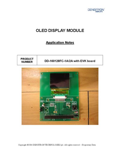
The document describes the EVK board schematic, timing characteristics for both 80‑series and 6800‑series MPU parallel interfaces, and the wiring connections required between the OLED display and the evaluation board. It also includes recommended initial code and sub‑functions for the 80‑series interface, enabling developers to quickly integrate the display.
Key sections cover the EVK schematic, detailed timing tables (address hold, setup, cycle times, pulse widths, and data timing), pin definitions, and example C code for initializing the display, setting memory pointers, and driving the RGB interface.
| Address hold time (tAH8) | 5 ns |
|---|---|
| Address setup time (tAS8) | 5 ns |
| System cycle (write) (tCYC8) | 100 ns |
| Write L pulse width | 4 ns |
| Data setup timing (tDS8) | 30 ns |
| System cycle (read) (tCYC8) | 200 ns |
The document provides sample initialization code that writes a series of command and data bytes (e.g., write_d(0x00); write_c(0x08); …) to set up the display.
Pins D17‑D9 constitute the 9‑bit bi‑directional data bus that connects to the MCU’s data bus.
Unused data pins should be grounded.