
The ADC122S655 is a dual 12-bit, 200 kSPS to 500 kSPS simultaneous sampling Analog-to-Digital (A/D) converter. It utilizes a successive-approximation register architecture to maintain the differential nature of the analog inputs throughout the conversion process, providing excellent common-mode signal rejection. The ADC122S655 features an external reference voltage that can be adjusted from 1.0V to VA. Its serial data output is in binary 2's complement format and compatible with various standards such as SPI™, QSPI™, MICROWIRE™, and common DSP serial interfaces. The ADC122S655 operates from a single 5V analog supply and consumes typically 11 mW of power at 500 kSPS. In power-down mode, the power consumption reduces to 3 µW. With its differential input, low power consumption, and compact size, the ADC122S655 is well-suited for direct connection to sensors in motor control applications. It is designed to operate reliably over the industrial temperature range of -40°C to +105°C and clock rates of 6.4 MHz to 16 MHz.
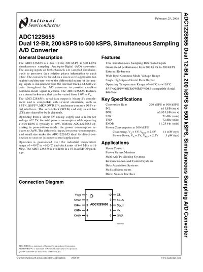
The ADC122S655 is a dual 12‑bit, 200 kSPS to 500 kSPS simultaneous‑sampling analog‑to‑digital converter with differential inputs and an external reference. It operates from a single 5 V analog supply and offers low power consumption (11 mW at 500 kSPS, 3 pW in power‑down mode).
The device is specified for an industrial temperature range of –40 °C to +105 °C, supports SPI, QSPI, and Microwire serial interfaces, and is supplied in a 10‑lead MSOP package. Detailed electrical characteristics, timing diagrams, and pin descriptions are provided for design integration.
| Conversion Rate | 200 kSPS to 500 kSPS |
|---|---|
| Integral Non‑Linearity (INL) | +1 LSB (max) |
| Differential Non‑Linearity (DNL) | +0.95 LSB (max) |
| Signal‑to‑Noise Ratio (SNR) | 71 dB (min) |
| Total Harmonic Distortion (THD) | -72 dB (min) |
| Effective Number of Bits (ENOB) | 11.25 bits (min) |
| Analog Supply Voltage | 4.5 V to 5.5 V |
| Clock Frequency Range | 6.4 MHz to 16 MHz |
The converter supports conversion rates from 200 kSPS up to 500 kSPS.
The device operates from a single analog supply of 4.5 V to 5.5 V.
The ADC is guaranteed to operate from –40 °C to +105 °C.