
The LMV851/LMV852/LMV854 are National’s low power, CMOS input, EMI hardened operational amplifiers. They offer low input bias current, a wide temperature range of -40 °C to +125 °C and exceptional performance, making them robust general purpose parts. Additionally, the LMV851/LMV852/LMV854 are EMI hardened to minimize any interference so they are ideal for EMI sensitive applications. The unity gain stable LMV851/LMV852/LMV854 feature 8 MHz of bandwidth while consuming only 0.4 mA of current per channel. These parts also maintain stability for capacitive loads as large as 200 pF. The LMV851/LMV852/ LMV854 provide superior performance and economy in terms of power and space usage. This family of parts has a maximum input offset voltage of 1 mV, a rail-to-rail output stage and an input common-mode voltage range that includes ground. Over an operating supply range from 2.7V to 5.5V the LMV851/LMV852/LMV854 provide a CMRR of 92 dB, and a PSRR of 93 dB. The LMV851/LMV852/LMV854 are offered in the space saving 5-Pin SC70 package, the 8-Pin MSOP and the 14-Pin TSSOP package.
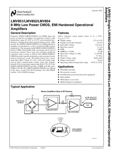
The LMV851, LMV852, and LMV854 are low‑power CMOS input operational amplifiers with a wide temperature range of –40 °C to +125 °C and EMI‑hardening for sensitive applications. They are offered in 5‑Pin SC70, 8‑Pin MSOP, and 14‑Pin TSSOP packages and operate from 2.7 V to 5.5 V supply voltage.
Key specifications include a 0.4 mA supply current per channel, 1 mV maximum input offset voltage, 0.1 pA input bias current, 8 MHz gain‑bandwidth product, rail‑to‑rail output swing, and up to 30 mA output drive. The devices provide 92 dB CMRR, 93 dB PSRR, and EMI rejection up to 89 dB at 1.8 GHz, making them suitable for photodiode preamps, piezo sensors, portable equipment, and medical diagnostics.
| Supply voltage range | 2.7 V to 5.5 V |
|---|---|
| Supply current per channel | 0.4 mA |
| Input offset voltage | 1 mV max |
| Gain‑bandwidth product (GBW) | 8 MHz |
| Output voltage swing | Rail‑to‑Rail |
| Output current drive | 30 mA |
| Operating temperature range | -40 °C to 125 °C |
| CMRR | 92 dB |
| PSRR | 93 dB |
The devices operate from 2.7 V up to 5.5 V.
Each channel consumes about 0.4 mA of current.
The gain‑bandwidth product is 8 MHz.