
LMK01000/LMK01010/LMK01020 is a high performance clock buffer, divider and distributor that provides an easy way to divide and distribute high performance clock signals throughout the system. The device provides best-in-class noise performance and is designed to be pin-to-pin and footprint compatible with LMK03000/LMK02000 family of precision clock conditioners. The LMK01000/LMK01010/LMK01020 family features two programmable clock inputs (CLKin0 and CLKin1) that allow the user to dynamically switch between different clock domains. Each device features 8 clock outputs with independently programmable dividers and delay adjustments. The outputs of the device can be easily synchronized by an external pin (SYNC*).
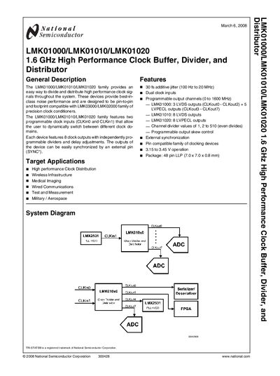
The LMK01000/LMK01010/LMK01020 family offers a high‑performance 1.6 GHz clock buffer, divider, and distribution solution with programmable clock inputs, independent output dividers, and selectable LVDS or LVPECL outputs. It targets applications such as wireless infrastructure, medical imaging, wired communications, test and measurement, and aerospace.
The document includes a general description, functional block and connection diagrams, pin descriptions, absolute maximum ratings, recommended operating conditions, electrical characteristics, clock distribution parameters, digital MICROWIRE interface timing, typical performance graphs, physical dimensions, and ordering information. It also contains legal notices and distributor contacts.
| Additive jitter | 30 fs (100 Hz to 20 MHz) |
|---|---|
| Power supply voltage (Vcc) | 3.15 V – 3.45 V |
| Package | 48‑pin LLP (7.0 × 7.0 × 0.8 mm) |
| Operating temperature (recommended) | -40 °C to 85 °C |
| Maximum clock input frequency | 1.6 GHz |
| Maximum divider value | 510 (even divides) |
The divider can be programmed from 1 up to 510, using only even divide values.
The recommended VCC range is 3.15 V to 3.45 V, with a typical value of 3.3 V.
The device is supplied in a 48‑pin lead‑less package (LLP).