
This document is about AD8110/AD8111 datasheet, which introduces the characteristics of the chip, including 16x8 high-performance non-blocking switch arrays, serial or parallel switch array control, serial data output, 150V load, 60MHz 0.1dB gain flatness, 0.02% differential gain error (RL = 150V), 0.028 differential phase error (RL = 150V), 260 MHz -3dB bandwidth, 500V/ms slew rate, 50mA low power, -78 dB all hostile crosstalk @5MHz, output disable, reset pin, 4000V human body model ESD rating etc.
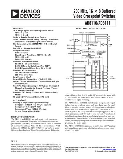
The AD8110 and AD8111 are high‑speed 16 × 8 video cross‑point switch matrices offering a -3 dB bandwidth greater than 260 MHz and channel switch times under 25 ns. They provide low crosstalk (‑78 dB at 5 MHz) and high isolation (‑97 dB at 5 MHz), with optional gain of +1 (AD8110) or +2 (AD8111). The devices support serial or parallel control, daisy‑chaining, and feature eight independent output buffers that can be disabled for high‑impedance operation.
Both parts are supplied in an 80‑lead LQFP package, operate from a +5 V supply while drawing only 50 mA idle current, and are rated for an industrial temperature range of –40 °C to +85 °C. They include ESD protection exceeding 4000 V human‑body model and provide a maximum output current of 40 mA per channel.
| -3 dB Bandwidth | 260 MHz |
|---|---|
| Slew Rate | 500 V/ms |
| Supply Current (AVCC, outputs enabled, no load) | 38 mA |
| Output Current | 40 mA |
| Gain (AD8110) | +1 |
| Gain (AD8111) | +2 |
The devices operate from 4.5 V to 5.5 V supply voltage.
Each output can source up to 40 mA.
Both parts are available in an 80‑lead plastic LQFP package (12 mm × 12 mm).
They have an ESD rating that exceeds 4000 V human‑body model.