
This document is the official datasheet of AD75019, which introduces the features of the product, including 256 switch arrays, wide signal range, low switch resistance, TTL/CMOS/microprocessor-compatible control lines, serial input simplifies interface, serial output allows cascading for more channels, low power consumption, etc.
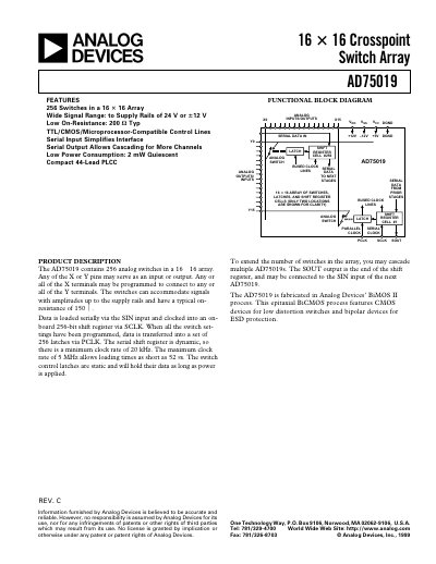
The AD75019 is a 16 × 16 crosspoint switch array containing 256 analog switches that can be programmed to connect any X pin to any Y pin. It operates over a wide signal range up to the supply rails and features a typical on‑resistance of 150 Ω. Data is loaded serially via SIN and clocked into a 256‑bit shift register, then transferred to parallel latches with PCLK. The device can be cascaded for larger arrays using the SOUT output.
Key specifications include a minimum clock rate of 20 kHz, a maximum clock rate of 5 MHz, supply voltage ranges of 9.0‑25.2 V (analog) and 4.5‑5.5 V (digital), and an operating temperature range of –25 °C to +85 °C. Proper power‑supply sequencing and bypass capacitors (0.1 mF ceramic) are required to ensure reliable operation.
| Switch ON Resistance (VDD/VSS = –12 V) | 150 Ω (typ) |
|---|---|
| Switch ON Resistance (VDD/VSS = –5 V) | 300 Ω (typ) |
| Leakage Current (VSIGNAL = –10 V) | 10 nA (typ) |
| Input/Output Capacitance | 25 pF |
| Maximum Clock Rate | 5 MHz |
| Minimum Clock Rate | 20 kHz |
| Power Dissipation (Absolute Max) | 1.0 W |
The typical on‑resistance is 150 Ω when VDD and VSS are –12 V.
They can be cascaded by connecting the SOUT output of one device to the SIN input of the next.