
ADV3200/ADV3201 32 × 32 Buffered Analog Crosspoint Switch is a switch array chip produced by Analog Devices, supporting single 5V, dual ±2.5V, dual ±3.3V power supply, with 60MHz, 0.1dB gain flatness, 0.1% differential gain error (RL = 150 Ω), 0.1° differential phase error (RL = 150 Ω), >300MHz bandwidth, >400V/μs slew rate, 1.25W power consumption, and -48dB @ 5MHz suppression ratio
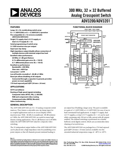
The ADV3200 and ADV3201 are 32 × 32 buffered analog crosspoint switch matrices designed for high‑speed video routing and signal handling. They offer selectable gain (+1 or +2), a single 5 V or dual ±2.5 V/±3.3 V supply options, and low power consumption of 1.25 W. Key features include a non‑blocking switch array, on‑screen‑display (OSD) insertion mux, sync‑tip clamp, and excellent video performance with 0.1 dB gain flatness to 60 MHz.
The document lists detailed specifications such as bandwidth >300 MHz, slew rate >400 V/µs, crosstalk –48 dB at 5 MHz, and operating temperature range –40 °C to +85 °C. It also provides pin‑out tables, timing diagrams for serial programming, power dissipation data, and application notes for CCTV, composite video, and high‑speed signal routing.
| Bandwidth | >300 MHz |
|---|---|
| Slew Rate | >400 V/µs |
| Power Consumption (Low Power) | 1.25 W |
| Operating Temperature Range | –40 °C to +85 °C |
| Input Capacitance | 3 pF |
| Output Impedance (Enabled) | 0.15 Ω |
| Crosstalk (Hostile, 5 MHz) | –48 dB |
| Gain Flatness | 0.1 dB at 60 MHz |
They can be powered from a single 5 V supply, dual ±2.5 V supplies, or dual ±3.3 V supplies (for the ADV3201 gain‑+2 version).
The device achieves –48 dB hostile crosstalk at 5 MHz with a 150 Ω load.
The parts are rated for operation from –40 °C up to +85 °C.