
the tps1100 is a single p-channel enhancement-mode mosfet from ti company. it is suitable for 3v or 5v power distribution and has low rDS(on), low vGS(th), and TTL and CMOS compatible inputs. it can be used in battery management systems, pulse-width modulated controllers or motor/bridge drivers.
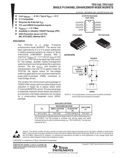
The TPS1100 and TPS1100Y are single P‑channel enhancement‑mode MOSFETs optimized for low‑voltage, battery‑powered systems. They feature low on‑resistance, fast switching (typical 10 ns rise time) and ESD protection up to 2 kV, making them suitable for high‑side switches in PWM controllers, motor‑bridge drivers, and other low‑voltage applications.
The devices are offered in two ultrathin packages: a D‑type SOIC and a PW‑type TSSOP. Both packages are available in taped‑and‑reeled form, with the PW version identified by the LE suffix. Detailed electrical characteristics, absolute maximum ratings, and typical performance graphs are provided in the document.
| Maximum drain‑to‑source voltage (VDS) | -15 V |
|---|---|
| Maximum gate‑to‑source voltage (VGS) | -15 V |
| Continuous drain current (150 °C) | 1 A |
| Storage temperature range | -55 °C to 150 °C |
| Operating junction temperature range | -40 °C to 150 °C |
| Typical total gate charge (Qg) | 5.45 nC |
The device can tolerate a drain‑to‑source voltage of up to –15 V and a gate‑to‑source voltage of up to –15 V.
The typical total gate charge is 5.45 nC.
The device is rated for operation from –40 °C to 150 °C junction temperature and can be stored from –55 °C to 150 °C.