
The TPS1120 is a dual p-channel enhancement-mode MOSFET with a maximum VGS(th) of -1.5V and an IDSS of only 0.5µA, making it the ideal high-side switch for low-voltage portable battery-management systems.
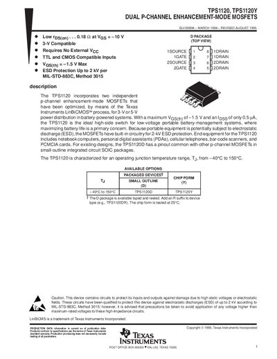
The TPS1120 and TPS1120Y are dual p‑channel enhancement‑mode MOSFETs optimized for low‑voltage battery‑powered systems. They feature built‑in ESD protection up to 2 kV and are suitable for high‑side switching in portable devices such as notebooks, PDAs, and cellular phones.
The document provides absolute maximum ratings, electrical characteristics, switching performance, typical on‑state resistance curves, and packaging options, along with ordering information and regulatory notices.
| Drain‑to‑source voltage (VDS) | -15 V |
|---|---|
| Operating junction temperature range (Ty) | -40 °C to 150 °C |
| Continuous drain current (Id) at 150 °C | 0.74 A |
| Total gate charge (Qg) | 5.45 nC |
| Static on‑state resistance (RDS(on)) at VGS = -3 V | 46 mΩ |
The MOSFETs are rated for a maximum drain‑to‑source voltage of -15 V.
The device operates from -40 °C up to 150 °C junction temperature.
The total gate charge is specified as 5.45 nC.
At a junction temperature of 150 °C, the continuous drain current is 0.74 A.