
The TPS2014 and TPS2015 power distribution switches are intended for applications where heavy capacitive loads and short circuits are likely to be encountered. The high-side switch is a 95-mΩ n-channel MOSFET. The switch is controlled by a logic enable that is compatible with 3-V and 5-V logic. Gate drive is provided by an internal charge pump designed to control the power switch rise times and fall times to minimize current surges during switching. The charge pump requires no external components and allows operation from supplies as low as 4 V. When the output load exceeds the current-limit threshold or a short is present, the TPS20xx limits the output current to a safe level by switching into a constant-current mode, and the overcurrent logic output is set to low. Continuous heavy overloads and shorts will set the overcurrent logic output to low.
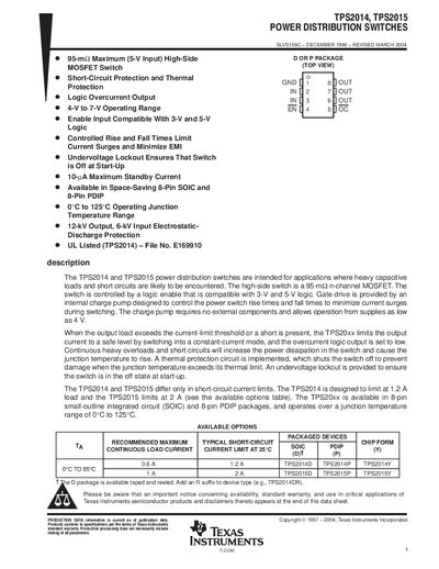
The TPS2014 and TPS2015 are high‑side power distribution switches designed for heavy capacitive loads and short‑circuit conditions. They feature a 95‑mΩ n‑channel MOSFET, internal charge‑pump driver, and logic‑compatible enable input (3 V‑5 V). The devices include over‑current, thermal, and undervoltage protection to ensure safe operation.
Both parts are offered in 8‑pin SOIC and 8‑pin PDIP packages and operate over a junction temperature range of 0 °C to 125 °C. Detailed electrical characteristics, absolute maximum ratings, and mechanical dimensions are provided for system designers.
| On‑State Resistance (RDS(on)) | 95 mΩ (typical at VJ=5.5 V, TJ=25 °C) |
|---|---|
| Input Voltage Range | 4 V to 5.5 V (typical) |
| Undervoltage Lockout Low‑Level Input Voltage | 3.2 V |
| Package Options | 8‑pin SOIC and 8‑pin PDIP |
When an overload or short occurs, the device limits the output current and asserts the OC output low until the fault is cleared.
Both parts are offered in 8‑pin SOIC and 8‑pin PDIP packages.