
This document introduces the FQPF47P06 P-Channel MOSFET produced by Fairchild. The device utilizes advanced DMOS technology, featuring low on-state resistance, superior switching performance, and the ability to withstand high energy pulses. It is suitable for low voltage applications such as automotive, DC/DC converters, and high efficiency switching for power management in portable and battery operated products.
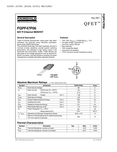
The FQPF47P06 is a P‑Channel enhancement mode power MOSFET designed for low‑voltage applications such as automotive DC/DC converters and portable power management. It features a low gate charge (typical 84 nC), low output capacitance, and robust avalanche and dv/dt performance.
Key specifications include a -60 V drain‑source rating, -30 A continuous drain current at 25 °C (‑21.2 A at 100 °C), 62 W power dissipation at 25 °C, and a maximum junction temperature of 175 °C. The device is supplied in a TO‑220F package with thermal resistance values of 2.42 °C·W (junction‑to‑case) and 62.5 °C·W (junction‑to‑ambient).
| Drain-Source Voltage (VDS) | -60 V |
|---|---|
| Continuous Drain Current (ID) @ 25°C | -30 A |
| Pulsed Drain Current (ID) (Note 1) | -120 A |
| Gate-Source Voltage (VGS) | +25 V |
| Power Dissipation (PD) @ 25°C | 62 W |
| Junction-to-Case Thermal Resistance (RθJC) | 2.42 °C·W |
| Junction-to-Ambient Thermal Resistance (RθJA) | 62.5 °C·W |
| Maximum Junction Temperature | 175 °C |
| Typical Gate Charge (Qg) | 84 nC |
The device can handle a continuous drain current of -30 A at 25 °C.
The maximum power dissipation is 62 W when the junction temperature is 25 °C.
The MOSFET is rated for a maximum junction temperature of 175 °C.
The typical gate charge is 84 nC.