
The IDT54/74FCT827AT/BT/CT/DT and IDT54/74FCT2827AT/BT/CT are high-performance CMOS buffers for military and commercial temperature ranges. They are built using an advanced dual metal CMOS technology and provide high-performance bus interface buffering for wide data/address paths or buses carrying parity. The buffers have NAND-ed output enables for maximum control flexibility and are designed for high-capacitance load drive capability and low-capacitance bus loading. The FCT2827T has balanced output drive with current limiting resistors, reducing ground bounce, undershoot, and the need for external series terminating resistors.
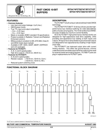
The IDT54/74FCT series provides 10‑bit CMOS bus buffers with low input leakage, true TTL compatibility, and high‑drive output options. Available in multiple packages (DIP, SOIC, SSOP, QSOP, CERPACK, LCC) and in radiation‑tolerant or radiation‑enhanced versions, the devices are suitable for both commercial and military applications.
Key features include selectable speed grades, high‑drive outputs (up to –15 mA IOH, 48 mA IOL for the FCT827T), low‑capacitance loading, and robust temperature ranges. Electrical characteristics, pin configurations, and switching parameters are detailed for design integration.
| Typical high‑level output voltage (VOH) | 3.3 V |
|---|---|
| Typical low‑level output voltage (VOL) | 0.3 V |
| High‑drive output current (FCT827T) | -15 mA IOH, 48 mA IOL |
| Commercial temperature range | 0 °C to +70 °C |
| Military temperature range | -55 °C to +125 °C |
The typical high‑level output voltage (VOH) is 3.3 V.
The FCT827T provides high‑drive outputs of –15 mA IOH and 48 mA IOL.