
MC14069UB is a 6-channel NMOS inverter, which supports a supply voltage range of 3.0V to 18V. It can drive low-power TTL loads or low-power Schottky TTL loads over the rated temperature range. It meets JEDEC UB specifications and has lead and lead-free packages available.
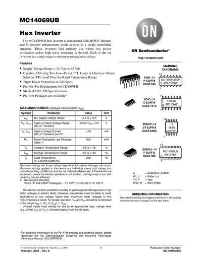
The MC14006UB hex inverter is a MOS P‑channel and N‑channel enhancement‑mode device packaged in a six‑inverter monolithic structure. It is intended for low‑power dissipation and high noise‑immunity applications, offering triple diode protection on all inputs and pin‑for‑pin compatibility with the CD4069UB.
The document includes detailed electrical characteristics, maximum ratings, pin assignments, logic diagrams, package dimensions for PDIP‑14, SOIC‑14, TSSOP‑14 and SOEIAJ‑14 packages, and ordering information. It also provides typical propagation delay and rise/fall times for various supply voltages.
| Supply Voltage Range | 3.0 Vdc to 18 Vdc |
|---|---|
| Power Dissipation (per package) | 500 mW |
| Input/Output Current per Pin | ±10 mA (DC or transient) |
The device operates from 3.0 Vdc up to 18 Vdc.
The MC14069UB contains six independent inverters.
The maximum power dissipation is 500 mW per package.