
The CDC3S04 is a four-channel low-power low-jitter sine-wave clock buffer. It can be used to buffer a single master clock to multiple peripherals. The four outputs (CLK1-CLK4) are designed for minimal channel-to-channel skew and ultralow additive output jitter. Each output has its own clock request inputs which enable the dedicated clock output. These clock requests are active-high (can also be changed to be active-low via I2C), and an output signal is generated that can be sent back to the master clock to request the clock (MCLK_REQ). MCKL_REQ is an open-source output and supports the wired-OR function (default mode)
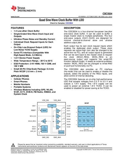
The CDC3S04 quad sine‑wave clock buffer provides 1:4 low‑jitter clock distribution with individual clock‑request inputs for each output. It operates from two 1.8 V supplies (core and analog) and includes an on‑chip low‑dropout regulator that can power an external 1.8 V TCXO.
Typical applications include cellular phones, smart phones, wireless modems, GPS, WLAN, Wi‑MAX and other portable or wireless systems that require low‑phase‑noise clock distribution.
| Battery supply voltage range | 0.5 V – 6.5 V |
|---|---|
| Operating temperature range | -30 °C – 85 °C |
| Storage temperature range | -65 °C – 150 °C |
| Continuous output current | 20 mA |
| Package | 0.4‑mm pitch WCSP (1.6 mm × 2 mm) |
| LDO output voltage | 1.8 V |
It is specified for operation from –30 °C to 85 °C.
It provides four independent sine‑wave clock outputs (CLK1‑CLK4).
Each output can source up to 20 mA continuous current.