
SPI21N10 SPP21N10,SPB21N10 SIPMOS Power-Transistor Product Summary is a N-Channel Enhancement mode power transistor. Its maximum working voltage is 100V, maximum drain current is 21A, and maximum on-resistance is 80mΩ. Its working temperature range is -55~+175℃.
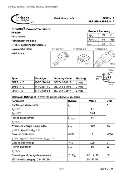
This document provides the preliminary electrical, thermal and dynamic characteristics of the Infineon SPI21N10 N‑channel power MOSFET, together with related devices SPP21N10 and SPB21N10. It includes maximum ratings, typical performance curves, and safety information for design engineers.
The sheet lists absolute maximum ratings, typical on‑state resistance, gate charge, avalanche energy, and operating temperature range, as well as detailed graphs for safe operating area, drain current, and transient thermal impedance. The information is intended for component selection and circuit design.
| Continuous drain current (Id) | 21 A |
|---|---|
| Maximum drain‑source voltage (Vds) | 100 V |
| Gate threshold voltage (Vgs(th)) typical | 2.1 V |
| On‑state resistance (Rds(on)) typical | 65 mΩ |
| Power dissipation (Pd) at 25 °C | 90 W |
| Operating temperature range | -55 °C to +175 °C |
| Thermal resistance, junction‑to‑case (RthJC) | 1.7 K/W |
The SPI21N10 can handle a continuous drain current of 21 A at 25 °C.
The device is rated for a maximum drain‑source voltage of 100 V.
The typical gate threshold voltage is 2.1 V.