
This data sheet provides detailed information on the MAX5062/MAX5063/MAX5064 high-frequency, 125V half-bridge, N-channel MOSFET drivers that drive high- and low-side MOSFETs in high-voltage applications. These drivers are independently controlled and their 35ns typical propagation delay, from input to output, are matched to within 3ns (typ).
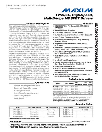
The MAX5062, MAX5063, and MAX5064 are 125 V, 2 A high‑speed half‑bridge MOSFET driver devices designed for telecom power converters, motor control, and other high‑frequency applications. They feature independent high‑side and low‑side drivers with typical propagation delays of 35 ns and programmable break‑before‑make timing.
The datasheet includes electrical characteristics, absolute maximum ratings, pin‑out tables for each device variant, package information for 8‑pin SO and 12‑pin thin QFN packages, and a selector guide that shows which driver configurations are non‑inverting, inverting, or mixed. Ordering information and contact details for Maxim Integrated Products are also provided.
| Maximum Input Voltage | 125 V |
|---|---|
| Typical Propagation Delay | 35 ns |
| Peak Source/Sink Current | 2 A |
| Operating Temperature Range | -40 °C to +125 °C |
| Logic Input Voltage Range (CMOS) | 8 V to 12.6 V (Vpp/2) |
The typical propagation delay from input to output is 35 ns.
The devices are rated for a maximum input voltage of 125 V.
They operate from –40 °C to +125 °C.