
MAX498/MAX499 are high-speed, quad/triple, single-pole/double-throw video switches with on-board closed-loop buffer amplifiers. The buffer amplifiers feature +6dB gain (AVCL = 2V/V), 250MHz -3dB bandwidth, 70MHz 0.1dB gain flatness, and 1250V/µs slew rate. Fast switching time (3ns) and fast settling time (12ns for a 4V step) make these devices excellent choices for a wide variety of video applications. The low differential gain/phase errors (0.03%/0.06°) and wide bandwidth make them ideal for both composite-video and RGB applications. The amplifiers are capable of delivering ±2.5V into back-terminated 50Ω or 75Ω cables, and they deliver ±2V to a 75Ω load, allowing multiple cables to be driven from a single output. For implementation of large switch arrays, a low-power disable mode places the amplifier outputs in a high- impedance state. Channel selection and output enable/disable are controlled by four TTL/CMOS- compatible logic inputs. Each video input is isolated by an AC-ground pin, which minimizes channel-to-channel capacitance and reduces crosstalk to 90dB at 10MHz. The four-channel MAX498 dissipates 390mW (typical) from ±5VDC power supplies with all output buffers enabled. Power consumption is reduced to 130mW with all buffers disabled. The corresponding dissipation for the three-channel MAX499 is 300mW enabled and 100mW disabled.
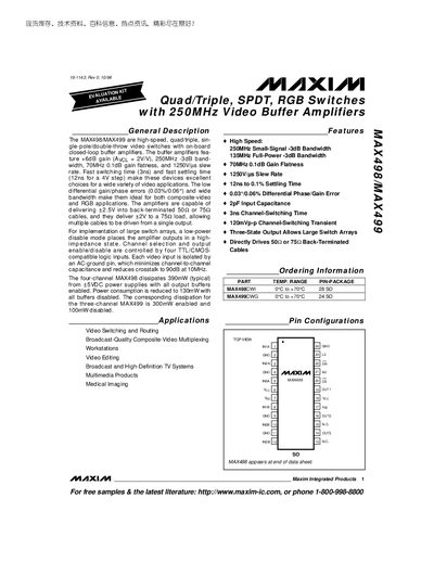
The MAX498 and MAX499 are high‑speed quad/triple SPDT video switches with on‑board closed‑loop buffer amplifiers. They provide +6 dB gain, 250 MHz small‑signal bandwidth, 12 ns settling time, and a 3 ns channel‑switching time, making them suitable for composite‑video, RGB, and high‑definition TV applications.
The datasheet includes absolute maximum ratings, DC and AC electrical characteristics, timing specifications, typical operating curves, pin descriptions, and package dimensions for both the 28‑pin SO (MAX498) and 24‑pin SO (MAX499) versions.
| Small‑signal -3 dB bandwidth | 250 MHz |
|---|---|
| Full‑power -3 dB bandwidth | 135 MHz |
| Gain flatness (0.1 dB) | 70 MHz |
| Slew rate | 1250 V/µs |
| Channel‑switching time | 3 ns |
| Settling time (0.1 % step) | 12 ns |
| Differential phase error | 0.06° |
| Input capacitance | 2 pF |
The channel‑switching time is typically 3 ns.
The small‑signal -3 dB bandwidth is 250 MHz.
The buffer amplifiers have a slew rate of 1250 V/µs.