
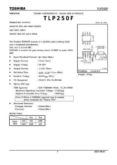
This document describes the Toshiba TLP250F GaAs phototransistor optocoupler, including its electrical characteristics, pin layout, and safety restrictions. The component is an 8‑lead DIP device intended for gate‑driving circuits of IGBT or power MOSFETs.
Key sections cover detailed specifications such as input threshold current, supply voltage, output current, isolation voltage, and mechanical parameters, as well as a pin‑configuration diagram, truth table, and recommended bypass capacitor. The final section outlines product‑use restrictions and handling precautions.
| Input Threshold Current | 5 mA (max) |
|---|---|
| Supply Voltage | 10 V ~ 35 V |
| Output Current | 1.5 A (max) |
| Switching Time | 0.5 µs (max) |
| Isolation Voltage | 2500 V (min) |
| Creepage Distance | 8.0 mm (min) |
| Clearance | 8.0 mm (min) |
| Weight | 0.54 g |
| UL Recognition | UL1577 |
| VDE Approval | DIN VDE0884/06.92 |
A 0.1 µF bypass capacitor should be connected between pin 8 and pin 5.
The device provides a minimum isolation voltage of 2500 V.
It operates with a supply voltage between 10 V and 35 V.