
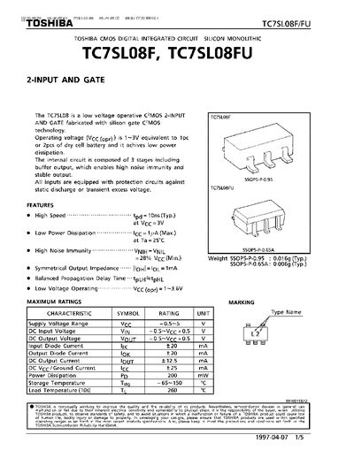
The TC7SLO8F/FU is a CMOS 2‑input AND gate fabricated with silicon‑gate C7MOS technology. It operates from 1 V to 3.6 V, offers low power dissipation, symmetrical output impedance and balanced propagation delay.
The device is supplied in SSOP5‑P‑0.95 and SSOP5‑P‑0.65A packages (typical weight 0.016 g and 0.006 g). Electrical specifications include a typical propagation delay of 10 ns, maximum output current of 1 A, and power dissipation of 200 mW. Recommended operating temperature is –40 °C to 85 °C.
| Supply Voltage (VCC) | 1 V ~ 3.6 V |
|---|---|
| Typical Propagation Delay | 10 ns |
| Maximum Output Current | 1 A |
| Power Dissipation | 200 mW |
| Storage Temperature | -65 °C ~ 150 °C |
The device operates from 1 V to 3.6 V supply voltage.
Typical propagation delay is 10 ns.