
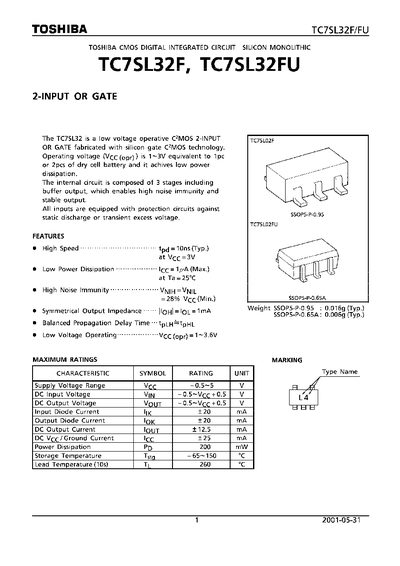
The TC7SL32F/FU is a low‑voltage CMOS 2‑input OR gate fabricated with silicon‑gate C?7MOS technology. It operates from 1 V to 3.6 V, offers low power dissipation, high noise immunity, and includes input protection against static discharge.
The device is offered in SSOP5‑P‑0.95 and SSOP5‑P‑0.65A packages with typical weights of 0.016 g and 0.006 g respectively. Maximum ratings include a supply voltage range of –0.5 V to 5 V, power dissipation of 200 mW, and specified temperature limits. The document also outlines recommended operating conditions, AC and DC electrical characteristics, and restrictions on product use.
| Supply Voltage (Vcc) | 1 V ~ 3.6 V |
|---|---|
| Power Dissipation (Pb) | 200 mW |
| Input Diode Current (ik) | ≤ 26 mA |
| Output Diode Current (Iout) | ≤ 20 mA |
| Storage Temperature (Tstg) | -65 °C ~ 150 °C |
The device operates with a supply voltage from 1 V to 3.6 V.
The maximum power dissipation is 200 mW.
Yes, the IC is not intended for safety‑critical or high‑reliability applications such as medical, aerospace, or traffic control equipment.