
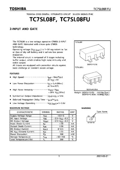
The TC7SLO8F/FU is a low‑voltage CMOS 2‑input AND gate with high noise immunity, low power dissipation, and symmetrical output impedance. It features protection circuits on all inputs and a three‑stage internal design that includes a buffer output for stable operation.
The document lists recommended operating conditions, DC and AC electrical characteristics, package dimensions for both SSOP5‑P‑0.95 and SSOP5‑P‑0.65A variants, and usage restrictions. It also includes maximum ratings, marking information, and handling guidelines for reliable integration into electronic designs.
| Operating voltage (Vcc) | 1 ~ 3.6 V |
|---|---|
| Typical output transition time (tTLH) | 5.0 ns |
| Power dissipation (Pb) | 200 mW |
| Package weight (SSOP5‑P‑0.95) | 0.016 g (typ.) |
| Storage temperature range | -65 °C ~ 150 °C |
| Input leakage current | ≤ 0.1 µA |
The device operates with a supply voltage (Vcc) from 1 V to 3.6 V.
The IC is recommended for operation between –40 °C and +85 °C.
Maximum power dissipation is specified as 200 mW.