
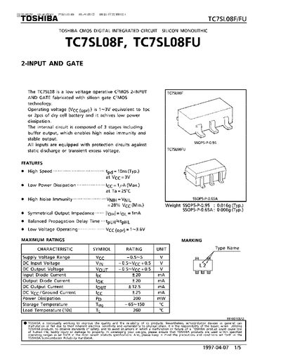
The TC7SLO8F/FU is a low‑voltage CMOS 2‑input AND gate fabricated with silicon‑gate CMOS technology. It operates from 1 V to 3.6 V supply voltage and offers low power dissipation, symmetrical output impedance, and high noise immunity. All inputs include protection against static discharge and transient over‑voltage.
The device is supplied in an SSOP‑5 package (0.95 mm or 0.65 mm pitch) with typical weight of 0.016 g (0.006 g for the smaller package). Electrical characteristics include a typical propagation delay of 75 ns, output transition times of 50 ns (min) to 90 ns (max), and a maximum power dissipation of 200 mW. Operating temperature range is –40 °C to 85 °C.
| Supply Voltage Range (Vec) | 1 V ~ 3.6 V |
|---|---|
| Operating Voltage (Vcc) | 1 V ~ 3 V |
| Power Dissipation (Pp) | 200 mW |
| Operating Temperature | -40 °C ~ 85 °C |
| Typical Propagation Delay (tPLH) | 75 ns |
| Typical Output Transition (tTLH) | 50 ns ~ 90 ns |
| Typical Weight (SSOP‑5, 0.95 mm) | 0.016 g |
| Typical Weight (SSOP‑5, 0.65 mm) | 0.006 g |
The device operates with a supply voltage (Vec) from 1 V to 3.6 V.
The typical propagation delay (tPLH) is 75 ns.
The maximum power dissipation is 200 mW.