
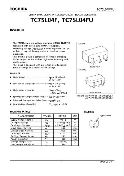
The TC7SLO4F/FU is a low‑voltage C7‑MOS inverter fabricated with silicon‑gate CMOS technology. It operates from 1 V to 3.6 V, offers low power dissipation, high noise immunity, and symmetrical output impedance.
The document provides detailed electrical characteristics, package dimensions, and usage restrictions for the SSOP5‑P‑0.95 and SSOP5‑P‑0.65A packages, along with recommended operating conditions and handling guidelines.
| Supply Voltage Range (VCC) | 1 ~ 3.6 V |
|---|---|
| Input Voltage (VIN) | 0 ~ VCC |
| Output Voltage (VOUT) | 0 ~ VCC |
| Power Dissipation (Pb) | 200 mW |
| Storage Temperature (Tstg) | -65 °C ~ 150 °C |
| Lead Temperature (TL, 10 s) | 260 °C |
| Typical Propagation Delay (tp_d) | 10 ns |
| Maximum Output Current (lec) | 14 A |
| Input Capacitance (Cin) | 5 ~ 10 pF |
| Package Weight (SSOP5‑P‑0.95) | 0.016 g (typ) |
The device is specified to operate from 1 V to 3.6 V.
Maximum power dissipation is 200 mW.
It can be stored between –65 °C and 150 °C.
Typical propagation delay is 10 ns.