
This document introduces the AD9212, an eight-channel ADC chip with features including 100 mW power consumption, 60.8 dB SNR, and excellent linearity. The chip utilizes a serial LVDS interface and supports low power mode and data frame outputs. It is suitable for applications such as medical imaging, portable ultrasound and digital beam forming systems, and quadrature radio receivers.
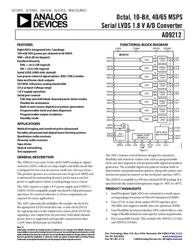
The AD9212 is an octal, 10‑bit analog‑to‑digital converter that operates up to 65 MSPS with a single 1.8 V supply. It integrates eight ADC channels in a compact 64‑lead LFCSP package and offers LVDS serial output, low‑power reduced‑signal options, and flexible SPI control.
The document provides full electrical specifications, timing diagrams, pin configurations, and typical performance data. It also lists applications such as medical imaging, ultrasound, radio receivers, tape drives, and test equipment, making it a comprehensive reference for designers.
| Resolution | 10 bits |
|---|---|
| Maximum Sampling Rate | 65 MSPS |
| Power per Channel | 100 mW at 65 MSPS |
| Input Voltage Range | 2 V p‑p differential |
| Supply Voltage | 1.8 V AVDD and DRVDD |
| Signal‑to‑Noise Ratio | 60.8 dB |
| Analog Bandwidth | 325 MHz |
| Total Power Dissipation (AD9212‑65) | 560 mW |
The AD9212 operates from a single 1.8 V supply for both AVDD and DRVDD.
The device can sample up to 65 MSPS.
Eight ADC channels are integrated into a single package.