
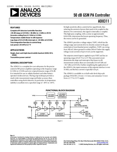
The AD8311 provides a complete low‑cost subsystem for precise control of RF power amplifiers in the 0.1 GHz to 2.5 GHz range, offering a 50 dB dynamic range and temperature‑stable linear‑in‑dB response. It is intended for cellular handsets and other battery‑operated wireless devices, delivering a voltage output (VAPC) that can directly drive gain‑control pins.
Key specifications include a supply voltage of 2.7 V‑5.5 V, quiescent current around 7.6 mA, and operation from –40 °C to +85 °C. The device features a set‑point input (VSET) of 0.25‑1.4 V, an output voltage swing of 150 mV‑3 V, and a low‑noise rail‑to‑rail buffer. Pin configuration, typical performance curves, and absolute maximum ratings are detailed in the document.
| Dynamic range (0.9 GHz) | 51 dB |
|---|---|
| Slope (0.9 GHz) | 23.6 mV/dB |
| Intercept (0.9 GHz) | –59.7 dBm |
| Supply voltage (VPOS) | 2.7 V to 5.5 V |
| Quiescent current | 7.6 mA (typical) |
| Operating temperature range | –40 °C to +85 °C |
The device can be powered with a supply voltage between 2.7 V and 5.5 V.
At 0.9 GHz the AD8311 provides a dynamic range of about 51 dB.