
This datasheet is a technical documentation of 256Mb x32 SDRAM product released by Micron Technology Inc. It details the product's features, options, packaging, operating temperature range, etc.
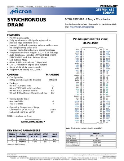
The MT48LC8M32B2 is a 256‑Mb (8 M × 32) synchronous DRAM organized as four banks with a fully synchronous, pipelined architecture. It operates from a single +3.3 V supply and supports CAS latencies of 1, 2 and 3, with programmable burst lengths of 1, 2, 4, 8 or a full page.
The datasheet provides detailed functional block diagrams, pin descriptions for 86‑pin TSOP and 90‑ball FBGA packages, timing tables, electrical characteristics, and command definitions for initialization, read/write, auto‑precharge, refresh and power‑down modes.
| Capacity | 256 Mb (8 M × 32) |
|---|---|
| Supply Voltage | +3.3 V ±0.3 V |
| CAS Latency | 1, 2, 3 |
| Burst Lengths | 1, 2, 4, 8, full page |
It operates from a single +3.3 V supply with a ±0.3 V tolerance.
The device supports CAS latency values of 1, 2, and 3.