
The AD6624A is part of Analog Devices’ SoftCell® multicarrier transceiver chipset designed for compatibility with Analog Devices’ family of high sample rate IF sampling ADCs (AD6640/ AD6644 12- and 14-bit). The SoftCell receiver comprises a digital receiver capable of digitizing an entire spectrum of carriers and digitally selecting the carrier of interest for tuning and channel selection. This architecture eliminates redundant radios in wireless base station applications. High dynamic range decimation filters offer a wide range of decimation rates. The RAM-based architecture allows easy reconfiguration for multimode applications. The decimating filters remove unwanted signals and noise from the channel of interest. When the channel of interest occupies less bandwidth than the input signal, this rejection of out-of-band noise is called “processing gain.” By using large decimation factors, this “processing gain” can improve the SNR of the ADC by 30 dB or more. In addition, the chipset includes a demodulator, IF filters, and ADC for receiving, demodulating, and digitizing RF signals.
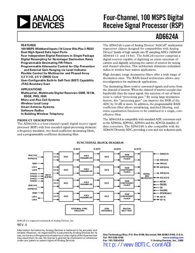
The AD6624A is a four‑channel (quad) digital receive signal processor (RSP) offering 100 MSPS wideband inputs, dual high‑speed data ports, and programmable decimating FIR filters. It provides flexible control for multicarrier and phased‑array applications and includes built‑in self‑test (BIST) and JTAG boundary‑scan capabilities.
The document lists electrical characteristics such as a typical VDD of 2.5 V and VDDIO of 3.3 V, CMOS/TTL logic compatibility, supply currents up to 545 mA at 100 MHz clock, and power dissipation up to 1.1 W. Detailed timing diagrams, pin functions, and microprocessor port timing for INM and MNM modes are also provided, along with package dimensions for the 196‑lead PBGA.
| Logic Input Compatibility | 3.3 V CMOS |
|---|---|
| Logic Output "1" Voltage | 2.4 V (typical) |
| Supply Current (CLK = 100 MHz) | 545 mA |
| Power Dissipation (CLK = 80 MHz) | 1.1 W |
| Maximum Serial Port Clock Frequency | 62.5 MHz |
Both the inputs and outputs are compatible with 3.3 V CMOS (and TTL for outputs).
The slave serial port’s SCLK operating frequency is limited to 62.5 MHz.
At a 100 MHz clock the supply current is 545 mA.