
The ADM1185 is an integrated, 4-channel, voltage monitoring and sequencing device.
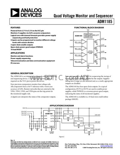
The ADM1185 is a quad‑channel voltage monitor and sequencing device that operates from 2.7 V to 5.5 V. It monitors up to four supply rails with 0.8 % accurate comparators and provides open‑drain enable outputs plus a power‑good output for sequencing and fault protection.
The device is supplied in a 10‑lead MSOP package and includes specifications for operating and absolute‑maximum ratings, thermal resistance, timing delays, and typical performance curves. Pin descriptions define four VIN inputs, three enable outputs, a PWRGD output, and the VCC supply pin.
| Operating Voltage Range (VCC) | 2.7 V to 5.5 V |
|---|---|
| Input Current (VINx) | ‑20 nA to +20 nA |
| Output Low Voltage (typical) | 0.4 V at VCC = 2.7 V, Isink = 2 mA |
| VIN1 to OUT1 Rising Delay (typical) | 190 ms |
| Absolute Maximum VCC Rating | ‑0.3 V to +6 V |
| Storage Temperature Range | ‑65 °C to +125 °C |
| Operating Temperature Range | ‑40 °C to +85 °C |
| Package | 10‑lead MSOP |
The device operates from 2.7 V to 5.5 V on the VCC pin.
Four inputs (VIN1‑VIN4) can be programmed to monitor separate voltage rails.
It provides an active‑high, open‑drain PWRGD output that goes low when any monitored rail falls below the threshold.
The typical rising delay is 190 ms.