
This document describes the features and characteristics of ADM1085/ADM1086/ADM1087/ADM1088 products, including programmable time delays, cascading with power modules for multiple supply sequencing, power supply monitoring, output stages, adjustable time delays, high voltage inputs and outputs, etc.
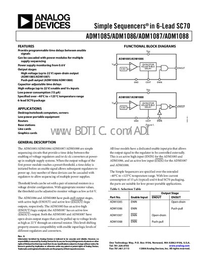
The ADM1087 (part of the ADM1085‑1088 family) is a simple sequencer that provides programmable time delays between enable signals for power‑up sequencing of multiple supplies. It offers high‑voltage open‑drain outputs, low power consumption, and can be cascaded for complex systems.
The document includes functional block diagrams, pin descriptions, electrical specifications, absolute maximum ratings, and typical performance curves, as well as ordering information and an evaluation board reference.
| Operating Voltage Range (VCC) | 2.25 V – 3.6 V |
|---|---|
| Vin Operating Voltage Range | 0 V – 22 V |
| Vin Hysteresis | 15 mV |
| CEXT Charge Current | 125 nA – 375 nA |
| Threshold Temperature Coefficient | 30 ppm/°C |
| Operating Temperature Range | -40 °C to +125 °C |
The ADM1087 uses an active‑low enable input (ENIN).
The open‑drain output can be pulled up to 22 V.
It operates from –40 °C to +125 °C.