
The document describes the functions and features of the AD7568 LC2MOS octal 12-bit DAC chip, including eight 12-bit DACs, four-quadrant multiplication, separate references, single +5V supply, and low power consumption. The chip has various applications in process control, automatic test equipment, and general-purpose instrumentation.
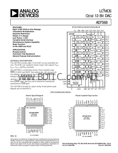
The AD7568 contains eight 12‑bit current‑output DACs in a single 44‑pin PQFP or PLCC package. It offers a single +5 V supply, low power consumption (≈1 mW), and a versatile serial interface with FSIN, CLKIN, and SDIN signals. The device supports simultaneous latch updates via the LDAC input and can be daisy‑chained using the SDOUT pin.
The document provides full electrical specifications, timing diagrams, pin descriptions, and example interfacing circuits for various microcontrollers and DSPs. It also includes ordering information, absolute maximum ratings, and typical performance curves for accuracy, noise, and dynamic behavior.
| Resolution | 12 bits |
|---|---|
| Relative Accuracy | +0.5 LSB max |
| Differential Nonlinearity | +0.9 LSB max |
| Supply Voltage Range | 4.75 V to 5.25 V |
| Input High Voltage | 2.4 V min |
| Input Low Voltage | 0.8 V max |
| Gain Temperature Coefficient | 2 ppm/°C typ |
| Storage Temperature Range | -65 °C to +150 °C |
The AD7568 contains eight 12‑bit DACs in one package.
The device provides a 12‑bit resolution.
When LDAC is taken low, all eight DAC latches are simultaneously updated with the contents of their input latches.
It operates from a single +5 V supply with a voltage range of 4.75 V to 5.25 V and a maximum power dissipation of 250 mW.