
AD9522-5 is a low phase noise, phase-locked loop (PLL) from Analog Devices. This chip supports external 3.3 V/5 V VCO/VCXO to 2.4 GHz, supports 1 differential or 2 single-ended reference inputs, accepts CMOS, LVPECL or LVDS references to 250 MHz, accepts 16.62 MHz to 33.33 MHz crystal as reference input, has an optional reference clock doubler, supports reference monitoring capability, has auto and manual reference switchover/holdover modes with selectable revertive/nonrevertive switching, glitch-free switchover between references, automatic recovery from holdover, supports digital or analog lock detect, optional zero delay operation. This chip has 12 800 MHz LVDS outputs, divided into 4 groups, each group of 3 has a 1-to-32 divider with phase delay. The additive broadband jitter is as low as 242 fs rms, grouped outputs channel-to-channel skew < 60 ps, each LVDS output can be configured as an independent output or connected to the PLL's internal 1-to-32 divider.
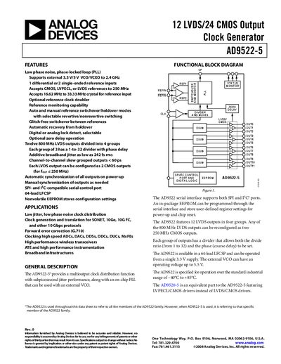
The AD9522-5 is a multi‑output clock generator offering 12 LVDS and up to 24 CMOS outputs with low phase‑noise PLL operation. It supports external VCO/VCXO inputs up to 2.4 GHz, automatic reference switchover, zero‑delay operation, and programmable output dividers for flexible frequency planning.
The document provides a functional block diagram, detailed pin descriptions, power‑supply requirements, PLL characteristics, timing diagrams, and extensive specifications such as phase‑noise performance, jitter, and output drive levels. Application notes cover high‑speed ADC clocking, frequency planning, and use of the ADIsimCLK modeling tool.
| Number of LVDS outputs | 12 |
|---|---|
| Supply voltage (VS) | 3.3 V ±5 % |
| Operating temperature range | -40 °C to +85 °C |
The device can be powered up to 5.25 V on the VCP pin.
Each LVDS output can be reconfigured as two 250 MHz CMOS outputs.