
This document describes a 12 LVDS/24 CMOS output clock generator with an integrated 2.8 GHz VCO. It features low phase noise, phase-locked loop (PLL), support for external 3.3 V/5 V VCO/VCXO, and various reference inputs.
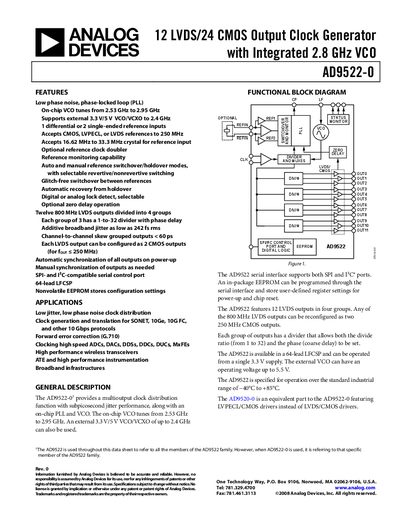
The AD9522-0 is a 12‑output LVDS/24‑output CMOS clock generator that includes an integrated 2.8 GHz on‑chip VCO. It offers low phase‑noise PLL operation, selectable reference inputs, zero‑delay modes, and both SPI and I²C serial control interfaces. The device is supplied in a 64‑lead LFCSP package and operates from a single 3.3 V supply.
The datasheet provides a full set of specifications, functional block diagrams, timing characteristics, and detailed register maps. It also includes application notes for clock distribution, high‑frequency clock generation, and guidance on LVDS/CMOS output termination and layout.
| LVDS Output Count | 12 |
|---|---|
| On‑chip VCO Frequency Range | 2.53 GHz – 2.95 GHz |
| Supply Voltage (VS) | 3.3 V ±5 % |
| Phase Noise @ 1 kHz Offset (LVDS) | ‑60 dBc/Hz |
| LVDS Output Rise Time (typ) | 150 ps |
The on‑chip VCO tunes from 2.53 GHz to 2.95 GHz.
The device provides twelve LVDS outputs (and can be reconfigured as twenty‑four CMOS outputs).
It operates from a single 3.3 V supply, with a tolerance of ±5 % (typical 3.3 V).
Typical LVDS rise and fall times are 150 ps to 350 ps.