
AD8323 is a low-cost, digitally controlled variable gain block that supports DOCSIS standard for reverse path transmission. It has a gain that can be programmed in 0.75 dB steps over a range of 53.5 dB, low distortion and output noise level -48 dBmV. It maintains a 75 ohm output impedance and supports SPI interfaces.
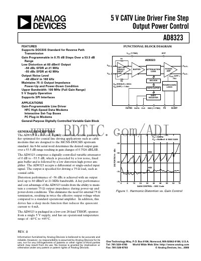
The AD8323 is a 5 V CATV line driver with digitally programmable gain for DOCSIS upstream applications. It offers a gain range of up to 53.5 dB in 0.75 dB steps, low distortion, and a constant 75 Ω output impedance that eliminates the need for external termination.
The document provides full electrical specifications, pin descriptions, timing requirements, layout guidelines, and an evaluation board bill of materials. It also explains SPI programming, power‑up/down behavior, and recommended circuit configurations for both single‑ended and differential inputs.
| Single‑Ended Input Resistance | 800 Ω |
|---|---|
| Differential Input Resistance | 1600 Ω |
| Input Capacitance | 2 pF |
| Gain Range | 52.5 – 54.5 dB |
| Gain Scaling Factor | 0.7526 dB/LSB |
| Bandwidth (All Gain Codes) | 100 MHz |
| Output Noise Spectral Density (Max Gain, 10 MHz) | -34 dBmV in 160 kHz |
| Power‑Up Quiescent Current | 123 – 133 mA |
| Power‑Down Quiescent Current | 30 – 35 mA |
| Sleep Mode Current | 2 – 4 mA |
| Operating Temperature Range | -40 °C to +85 °C |
| Supply Voltage Range | 4.75 V to 5.25 V |
Gain is set with an 8‑bit serial word over an SPI interface using the DATEN, SDATA, and CLK pins.
The device operates from a single 5 V supply with an acceptable range of 4.75 V to 5.25 V.
In sleep mode the quiescent current is reduced to about 4 mA.