
This data sheet describes the ADL5201, an integrated circuit for high-frequency digitally controlled VGA. The device has a wide dynamic range and high output power, making it suitable for use in a variety of applications, including differential ADC drivers, high IF sampling receivers, high output power IF amplifiers, and instrumentation.
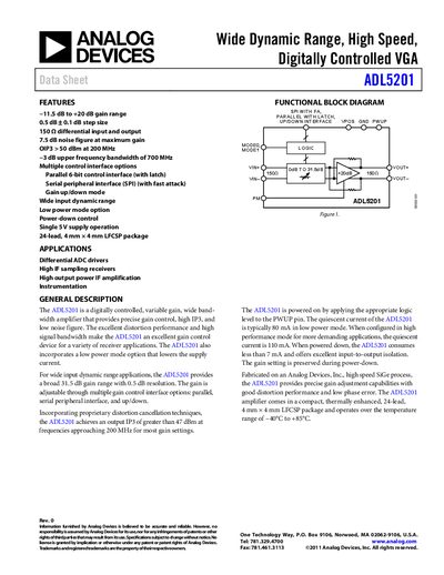
The ADL5201 is a digitally controlled, variable‑gain, wide‑bandwidth amplifier that offers precise gain control, high third‑order intercept (OIP3), and low noise figure. It operates from a single 5 V supply and includes multiple digital control interfaces.
Key features include a gain range of –11.5 dB to +20 dB with 0.5 dB steps, 700 MHz –3 dB bandwidth, 7.5 dB noise figure at maximum gain, and optional low‑power mode. The datasheet details pin functions, electrical ratings, typical performance curves, and evaluation‑board information.
| Gain range | –11.5 dB to +20 dB |
|---|---|
| Gain step size | 0.5 dB ± 0.1 dB |
| Bandwidth (‑3 dB) | 700 MHz |
| Noise figure (max gain) | 7.5 dB |
| Output IP3 (OIP3) | > 50 dBm at 200 MHz |
| Supply voltage | 4.5 V – 5.5 V |
| Quiescent current (high‑performance mode) | 110 mA |
| Quiescent current (low‑power mode) | 80 mA |
| Operating temperature range | –40 °C to +85 °C |
The ADL5201 provides a gain range from –11.5 dB to +20 dB.
The device powers up when a logic high is applied to the PWUP pin.
It supports parallel 6‑bit control with latch, a serial peripheral interface (SPI) with fast attack, and an up/down gain control mode.
The part operates from a supply voltage between 4.5 V and 5.5 V.