
This document describes the features and characteristics of the ADL5202 VGA, including wide dynamic range, high speed, and digital control.
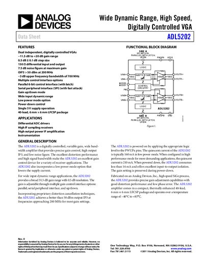
The ADL5202 from Analog Devices is a dual‑channel, digitally controlled variable‑gain amplifier designed for high‑performance receiver applications. It offers a wide gain range of −11.5 dB to +20 dB with 0.5 dB steps, a 700 MHz −3 dB bandwidth, and a low noise figure of 7.5 dB at maximum gain. The device supports multiple control interfaces, including a 6‑bit parallel bus, SPI, and up/down gain control, and includes a low‑power mode that reduces supply current.
The amplifier is supplied from a single 5 V source (4.5 V – 5.5 V) and operates over a temperature range of −40 °C to +85 °C. In high‑performance mode the quiescent current is 210 mA, while low‑power mode reduces it to 160 mA; power‑down current is less than 14 mA. Output performance includes an OIP3 greater than 50 dBm at 200 MHz and a 1 dB compression point of 19.5 dBm at 300 MHz.
| Gain range | -11.5 dB to +20 dB |
|---|---|
| Gain step size | 0.5 dB ± 0.1 dB |
| Bandwidth (−3 dB) | 700 MHz |
| Noise figure (max gain) | 7.5 dB |
| Output IP3 | > 50 dBm at 200 MHz |
| Supply voltage | 4.5 V – 5.5 V |
| Quiescent current (high‑performance mode) | 210 mA |
| Quiescent current (low‑power mode) | 160 mA |
| Operating temperature range | -40 °C to +85 °C |
The ADL5202 provides a gain range from –11.5 dB up to +20 dB.
The device operates from a single supply of 4.5 V to 5.5 V.
The ADL5202 achieves an OIP3 greater than 50 dBm at 200 MHz.