
The XC6411/XC6412 series is a dual LDO regulator manufactured using CMOS process. The series achieves very low supply current 0.8μ A typical by channel and consists of a reference voltage source, an error amplifier, a current foldback circuit, and a phase compensation circuit plus a driver transistor. The XC6411P series in SOT-25 packages, the XC6412B series in SOT-26 packages make high density mounting possible. Therefore, the series is ideally suited for applications where high density mounting is required such as mobile equipment. Each output voltage of two regulators VR1 and VR2 is selectable in 0.1V increments within a range of 0.9V to 5.0V by laser trimming. The series is compatible with low ESR ceramic capacitors, which provides stable outputs. The VR1 and VR2 are completely isolated so that a cross talk during load fluctuation is minimized. The current limiter's foldback circuit also operates as a short protection for the output pin.
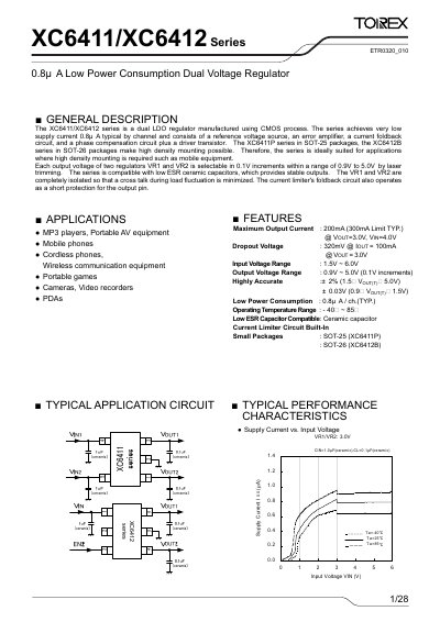
The XC6411/XC6412 series are dual low‑dropout (LDO) voltage regulators fabricated with a CMOS process. Each channel draws only 0.8 µA typical supply current and provides selectable output voltages from 0.9 V to 5.0 V in 0.1 V steps, making them suitable for high‑density mobile applications such as MP3 players, phones and portable AV equipment.
Two independent regulators (VR1 and VR2) are fully isolated, feature built‑in foldback current limiting, and are offered in compact SOT‑25 (XC6411P) and SOT‑26 (XC6412B) packages. The devices operate over a wide input range (1.5 V‑6.0 V) and an ambient temperature range of –40 °C to +85 °C.
| Maximum Output Current | 200 mA (300 mA limit) @ VOUT=3.0 V, VIN=4.0 V |
|---|---|
| Dropout Voltage | 320 mV @ IOUT=100 mA, VOUT=3.0 V |
| Input Voltage Range | 1.5 V ~ 6.0 V |
| Output Voltage Range | 0.9 V ~ 5.0 V (0.1 V increments) |
| Supply Current per Channel | 0.8 µA typical |
| Operating Temperature Range | -40 °C ~ +85 °C |
| Package Types | SOT‑25 (XC6411P) and SOT‑26 (XC6412B) |
The regulators can deliver up to 200 mA typical output current, with a 300 mA limit at VOUT = 3.0 V and VIN = 4.0 V.
The devices operate with an input voltage from 1.5 V to 6.0 V.
Each channel consumes about 0.8 µA typical supply current.
The XC6411P version is offered in an SOT‑25 package, while the XC6412B version uses an SOT‑26 package.