
XC6413/XC6414 series are highly precise, low noise, positive voltage LDO regulators with voltage detector manufactured using CMOS processes which features high ripple rejection and low dropout. The series is compased of a voltage reference, an error amplifier, a current limiter and a phase compensation circuit plus a driver transistor. Detect voltage is selectable in 0.1V increments within a range of 0.9V ~ 6.0V and VR output voltage is selectable within a range of 0.9V ~ 5.5V. The series is also compatible with low ESR ceramic capacitors which give added output stability. This stability can be maintained even during load fluctuations due to the excellent transient response of the series. The current limiter’s foldback circuit operates as a short-circuit protection as well as the output current limiter for the output pin. The series provides optional user selection for a variety of circuit applications such as detector monitoring, detector output logic, CE and EN pin input logic, internal pull-up/down resistors. The IC’s internal regulator circuit can be placed in stand-by mode via the EN function with the XC6413/14A to C series. The whole IC can be placed in stand-by mode, by placing EN pin input “high” level.
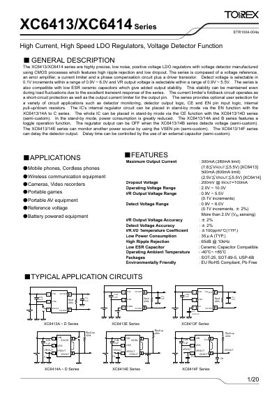
The XC6413/XC6414 series are high‑precision, low‑noise, positive‑voltage LDO regulators with built‑in voltage‑detect functions. They offer selectable output and detect voltages, high ripple rejection, and low dropout performance, and are compatible with low‑ESR ceramic capacitors for stable operation.
Key features include optional toggle, EN/CE standby functions, various logic input options, and customizable delay functions. The series is supplied in SOT‑25, SOT‑89‑5, and USP‑6B packages and complies with RoHS standards.
| Maximum Output Current (XC6413) | 300 mA (380 mA limit) |
|---|---|
| Dropout Voltage @ 100 mA | 200 mV |
| VR Output Voltage Range | 0.9 V ~ 5.5 V (0.1 V increments) |
| Detect Voltage Range | 0.9 V ~ 6.0 V (0.1 V increments) |
| Ripple Rejection (PSRR) @ 10 kHz | 65 dB |
| Operating Ambient Temperature | -40 °C ~ +85 °C |
| Power Dissipation (USP‑6B) | 100 mW |
The XC6413 series can deliver up to 300 mA (380 mA limit) when VROUT is between 1.8 V and 5.5 V.
The dropout voltage is specified as 200 mV at an output current of 100 mA.
Output voltage (VR) can be set from 0.9 V to 5.5 V in 0.1 V steps, and detect voltage (VDF) from 0.9 V to 6.0 V in the same increments.
The device provides a ripple rejection of 65 dB at 10 kHz.