
The XC6501 series is a high-speed, low-noise CMOS LDO regulator that can provide stable output voltages even without a load capacitor. This is possible because phase compensation is carried out internally unlike other LDOs where it is done externally. The series consists of a reference voltage source, driver transistor, error amplifier, current limit circuit, and phase compensation circuit. The CE function enables the circuit to be put into stand-by mode by inputting a low level signal to the CE pin thereby reducing current consumption from an already low 13μA (in operation) to less than 0.1μA. In the stand-by mode, if a CL capacitor is used, the electric charge stored at CL can be discharged via the internal auto-discharge switch and as a result, the VOUT pin quickly returns to the VSS level. The current limit fold-back circuit operates as a short circuit protection and a current limiter function for the output pin.
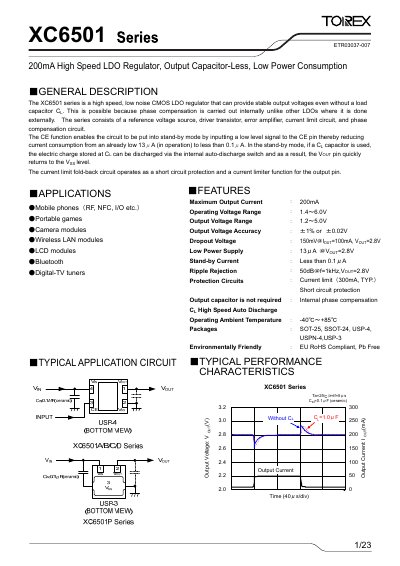
The XC6501 series is a high‑speed, low‑noise CMOS LDO regulator designed to provide stable output voltages without the need for an external output capacitor. It incorporates internal phase compensation, a current‑limit fold‑back circuit, and a standby mode that reduces quiescent current to below 0.1 µA.
Key features include a 200 mA maximum output current, wide operating voltage range (1.4‑6.0 V), selectable output voltages from 1.2‑5.0 V, and protection functions such as current limiting and short‑circuit protection. The device is offered in compact packages (SOT‑25, SSOT‑24, USP‑4, USPN‑4, USP‑3) and is suited for mobile phones, camera modules, wireless LAN, Bluetooth, and other portable electronics.
| Maximum Output Current | 200 mA |
|---|---|
| Operating Voltage Range | 1.4 V – 6.0 V |
| Output Voltage Range | 1.2 V – 5.0 V |
| Output Voltage Accuracy | ±1 % or ±0.02 V |
| Dropout Voltage | 150 mV @ IOUT=100 mA, VOUT=2.8 V |
| Quiescent Current (Normal) | 13 µA @ VOUT=2.8 V |
| Stand‑by Current | < 0.1 µA |
| Ripple Rejection | 50 dB @ 1 kHz |
| Package Types | SOT‑25, SSOT‑24, USP‑4, USPN‑4, USP‑3 |
| Output Capacitor Requirement | Not required |
The regulator can deliver up to 200 mA of output current.
No, the device operates without an external output capacitor thanks to internal phase compensation.
It includes a current‑limit circuit (typical 300 mA) and short‑circuit protection.
The standby current is less than 0.1 µA.