
The XC6505 series is a low power, high speed 200mA LDO regulator with an input voltage range of 1.7V to 10.5V, an output voltage range of 1.5V to 8.0V, an accuracy of ±1.0%(2.0V to 8.0V), a temperature stability of ±30ppm/℃, a dropout voltage of 190mV @ VOUT=3.3V, IOUT =100mA, a low power consumption of 5.5μA (TYP.), a chip enable (CE) of active high 0.1μA (standby), high ripple rejection: 60dB@1kHz, protection: current limiter (300mA, TYP.), short circuit protection.
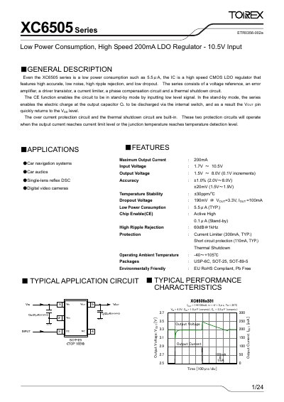
The XC6505 Series is a low‑power, high‑speed CMOS LDO regulator offering up to 200 mA output current with low dropout and high ripple rejection. It includes built‑in voltage reference, error amplifier, current limiter, thermal shutdown and optional chip‑enable functions.
The document provides detailed pin configurations, absolute maximum ratings, electrical characteristics, typical performance curves, packaging information and marking rules, along with recommended capacitor values and usage notes for reliable operation.
| Maximum Output Current | 200 mA |
|---|---|
| Input Voltage Range | 1.7 V – 10.5 V |
| Output Voltage Range | 1.5 V – 8.0 V (0.1 V increments) |
| Accuracy (2.0 V – 8.0 V) | ±1.0 % |
| Dropout Voltage (at 100 mA, 3.3 V out) | 190 mV |
| Low Power Consumption (typical) | 5.5 µA |
| Thermal Shutdown Detect Temperature | -150 °C |
| Package Options | USP‑6C, SOT‑25, SOT‑89‑5 |
The regulator can deliver up to 200 mA of output current.
It operates with an input voltage from 1.7 V to 10.5 V.
Stand‑by current is 0.1 µA when the CE pin is active high.
It includes over‑current protection, short‑circuit protection and an internal thermal‑shutdown circuit.