
The XC6229 series is a high-speed LDO regulator that features high accuracy, low noise, high ripple rejection, low dropout, and low power consumption. Housed in the ultra-small LGA-4B01 (0.75 x 0.75, h=0.3mm MAX.) package, the XC6229 is ideal for space-saving design. The XC6229 consists of a voltage reference, an error amplifier, a driver transistor, a current limiter, a phase compensation circuit, a thermal shutdown circuit, and an inrush current protection circuit. The CE function enables the circuit to be in standby mode by inputting a low-level signal. In standby mode, the series enables the electric charge at the output capacitor CL to be discharged via the internal switch, and as a result, the VOUT pin quickly returns to the VSS level. The output stabilization capacitor CL is also compatible with low ESR ceramic capacitors. The output voltage is selectable in 0.05V increments within the range of 1.2V to 4.0V, which is fixed by laser trimming technologies. The overcurrent protection circuit and the thermal shutdown circuit are built-in. These two protection circuits will operate in case of faults.
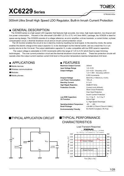
The XC6229 series is a high‑speed LDO regulator designed for space‑saving applications such as mobile devices, wireless communications, modules, and mobile phones. It integrates a voltage reference, error amplifier, driver transistor, current limiter, phase‑compensation, thermal shutdown, and inrush‑current protection in an ultra‑small LGA‑4B01 package.
Key features include a selectable output voltage from 1.2 V to 4.0 V in 0.05 V steps, maximum output current of 300 mA, dropout voltage as low as 80 mV at 150 mA, low standby current (0.1 µA), high ripple rejection (80 dB at 1 kHz), and multiple protection circuits (current limit, short‑circuit, over‑heat, inrush). The device operates from 1.6 V to 5.5 V input and is RoHS‑compliant.
| Maximum Output Current | 300 mA |
|---|---|
| Dropout Voltage | 80 mV @ IOUT=150 mA |
| Input Voltage Range | 1.6 V – 5.5 V |
| Stand‑by Current | 0.1 µA |
| Ripple Rejection | 80 dB @ 1 kHz |
The CE pin shuts down the IC’s internal circuitry and discharges the output capacitor, causing the VOUT pin to return to the VSS level.
The device includes current‑limit, short‑circuit, over‑heat, and inrush‑current protection circuits.
It is housed in an LGA‑4B01 package measuring 0.75 mm × 0.75 mm × 0.3 mm (max).
The output voltage can be set in 0.05 V increments from 1.2 V to 4.0 V.