
This document is a guide for converting existing linecard designs using Zarlink’s QSLAC™ devices to designs using the newer QLSLAC™ devices with a minimal amount of rework. The QLSLAC device is a low voltage and low power replacement for the QSLAC device. Because of the lower voltage, the analog output voltage is reduced compared to the QSLAC device, resulting in lower receive gains. Lower receive levels may be easily compensated in the Subscriber Line Interface Circuit. Zarlink recommends steps in this document that will allow full software compatibility with existing QSLAC device designs with only minor hardware modifications.
The document provides step‑by‑step instructions for redesigning line‑card circuits that currently use 5.0 V QSLAC devices so they can operate with 3.3 V QLSLAC devices. It details power‑supply considerations, interface timing changes, and required gain modifications to maintain performance.
Key sections include Power Supply Considerations, Interface Considerations (MPI, PCM, Master Clock, SLIC control), Subscriber Line Interface Circuit considerations, SLAC Coefficients, and Comparative Transmission Performance with example simulations.
| QSLAC supply voltage | +5.0 V digital and analog |
|---|---|
| QLSLAC supply voltage | +3.3 V |
| Minimum regulator current per QLSLAC device | 55 mA |
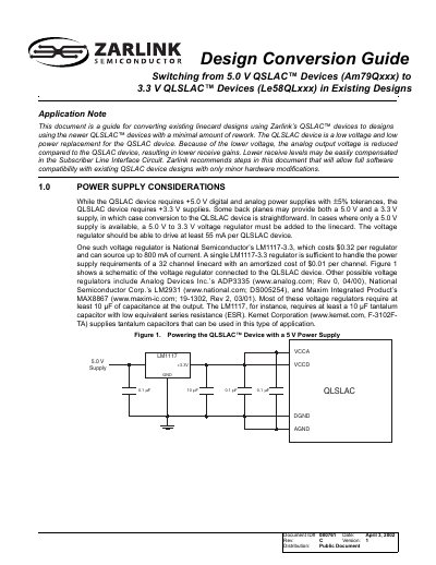
The document recommends National Semiconductor’s LM1117‑3.3 regulator, which can source up to 800 mA.
The pull‑up resistors should be reduced from 360 Ω to 240 Ω to maintain similar rise‑time.