
TC74LCX04F/FN/FT/FK is a high-performance CMOS inverter designed for use in 3.3V systems. It achieves high-speed operation while maintaining CMOS low power dissipation. The device is designed for low-voltage (3.3V) VCC applications, but it can also be used to interface with a 5V supply environment for inputs. All inputs are equipped with protection circuits against static discharge.
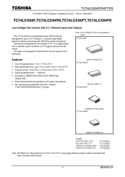
The TC74LCX04 family is a high‑performance CMOS hex inverter designed for 3.3‑V systems but compatible with 5‑V environments. It features low‑voltage operation (1.65‑3.6 V), high‑speed propagation (5.2 ns max), 24 mA output drive, and built‑in power‑down protection on all pins.
The device is offered in several JEDEC packages (SOP‑14, SOIC‑14, TSSOP‑14, VSSOP‑14) with typical weights ranging from 0.02 g to 0.18 g. Electrical characteristics include input capacitance of 7 pF, output capacitance of 8 pF, and a maximum power dissipation of 180 mW. Operating temperature is specified from –40 °C to 85 °C, and absolute maximum ratings allow supply voltages from 0.5 V to 7.0 V.
| Low‑voltage operation range | 1.65 V to 3.6 V |
|---|---|
| Propagation delay (tpd) | 5.2 ns (max) at VCC = 3.0‑3.6 V |
| Output current | 24 mA (min) at Voc = 3.0 V |
| Power‑down protection | Provided on all inputs and outputs |
| Operating temperature | -40 °C to 85 °C |
| Input capacitance (CIN) | 7 pF (typ) |
| Output capacitance (Cout) | 8 pF (typ) |
| Power dissipation (Pp) | 180 mW |
The typical propagation delay is 5.2 ns (maximum) when VCC is between 3.0 V and 3.6 V.
The device is offered in JEDEC SOP‑14, SOIC‑14, TSSOP‑14, and VSSOP‑14 packages.
The absolute maximum supply voltage (Voc) is 0.5 V to 7.0 V.
Yes, the inputs are 5‑V tolerant and the device can interface to a 5‑V supply environment.