
This file provides details on the TC7SZ08AFE, including its features, operating voltage range, input voltage, output voltage, input diode current, output diode current, output current, input current, power dissipation, storage temperature, lead temperature, etc.
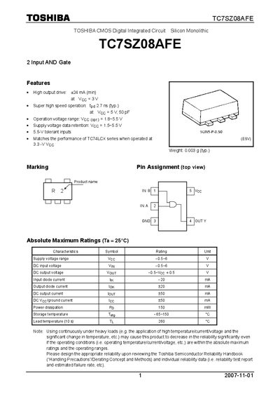
The TC7SZO8AFE is a CMOS digital integrated circuit that implements a 2‑input AND function. It offers high output drive up to +24 mA (min) and a typical propagation delay of 2.7 ns. The device operates from a supply voltage range of 1.8 V to 5.5 V and is designed for low‑power, high‑speed applications.
The datasheet includes absolute maximum ratings, electrical and AC characteristics, package dimensions, and important restrictions on product use. Users are advised to follow Toshiba’s Semiconductor Reliability Handbook for handling and derating recommendations, and to avoid use in safety‑critical or high‑reliability systems.
| High output drive | +24 mA (min) |
|---|---|
| Propagation delay (typical) | 2.7 ns |
| Input voltage range | 0 V ~ 5.5 V |
| Output voltage range | 0 V ~ Vcc |
| Operating temperature range | -40 °C ~ 85 °C |
| Weight | 0.003 g (typ.) |
| Power dissipation | 150 mW |
The device can be supplied up to 5.5 V (absolute maximum rating).
The typical propagation delay is 2.7 ns.
Yes, it should not be used in safety‑critical applications such as medical instruments, aerospace, or any equipment where failure could cause loss of life.
Refer to the Toshiba Semiconductor Reliability Handbook for handling precautions and derating concepts.